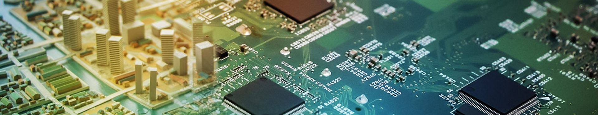
In the vast ecosystem of electronic design, few components offer the combination of versatility, reliability, and cost-effectiveness found in the Double-sided Board. While complex multilayer and HDI technologies capture headlines, the Double-sided Board remains the workhorse of countless applications—from industrial controls and power supplies to consumer electronics and automotive systems. HONTEC has built a strong reputation as a trusted manufacturer of Double-sided Board solutions, serving high-tech industries across 28 countries with specialized expertise in high-mix, low-volume, and quick-turn prototype production.
The enduring value of the Double-sided Board lies in its elegant simplicity. By placing copper traces on both sides of the substrate and connecting them through plated through-holes, this construction doubles the routing capacity of single-sided boards while maintaining straightforward manufacturing processes. For countless applications that require moderate component density, reliable performance, and predictable cost structures, the Double-sided Board delivers the ideal balance of capability and value.
Located in Shenzhen, Guangdong, HONTEC combines advanced manufacturing capabilities with rigorous quality standards. Every Double-sided Board produced carries the assurance of UL, SGS, and ISO9001 certifications, while the company actively implements ISO14001 and TS16949 standards to meet the demanding requirements of automotive and industrial applications. With logistics partnerships that include UPS, DHL, and world-class freight forwarders, HONTEC ensures that prototype and production orders reach destinations worldwide efficiently. Every inquiry receives a response within 24 hours, reflecting a commitment to responsiveness that global engineering teams value.
The choice between a Double-sided Board and other constructions depends on the specific requirements of the application. Single-sided boards place copper traces on only one surface, limiting routing options and typically requiring jumper wires for circuits that must cross. A Double-sided Board adds copper on both sides, connected by plated through-holes that allow traces to transition between layers. This doubles the available routing area and eliminates the need for jumpers, enabling more compact designs and cleaner layouts. Multilayer boards add additional internal layers, offering even higher density but at increased cost and longer lead times. HONTEC recommends a Double-sided Board for designs with moderate component counts, mixed analog and digital sections that benefit from separate ground planes, or applications where cost efficiency is a primary consideration. For designs requiring more than two signal layers or complex impedance control, multilayer construction becomes necessary. The engineering team at HONTEC provides guidance during the design review phase, helping clients evaluate factors such as component density, signal integrity requirements, and production volume to determine the optimal construction for their specific application.
Plated through-holes represent the critical interconnection feature in any Double-sided Board, as they provide the electrical pathway between top and bottom layers while also serving as mechanical anchors for component leads. HONTEC implements a comprehensive process control system to ensure through-hole reliability. The process begins with precision drilling using carbide bits that maintain hole diameter tolerances within ±0.05mm. Following drilling, a desmear process removes any debris and prepares the hole walls for copper deposition. Electroless copper plating creates a thin conductive layer across the hole walls, followed by electrolytic copper plating that builds up to the specified thickness, typically 0.025mm or greater. HONTEC conducts destructive cross-section analysis on every production batch, allowing visual inspection of copper thickness distribution, plating uniformity, and interface integrity. Thermal stress testing simulates assembly conditions by subjecting the Double-sided Board to multiple reflow cycles, with continuity testing performed between cycles to detect any via cracking or separation. For designs with particularly high reliability requirements, HONTEC offers enhanced plating processes and additional testing protocols. This systematic approach to through-hole quality ensures that the Double-sided Board maintains electrical continuity and mechanical integrity throughout its operational life.
HONTEC employs a multi-stage testing protocol to verify that every Double-sided Board meets design specifications before shipment. Electrical testing forms the foundation of quality verification, utilizing flying probe or fixture-based test systems to confirm continuity for every net and isolation between adjacent nets. For Double-sided Board designs with impedance-critical traces, time-domain reflectometry testing verifies that characteristic impedance falls within specified tolerances. Automated optical inspection scans the entire board surface to detect defects such as shorts, opens, insufficient solder mask coverage, or trace irregularities that might escape electrical testing. Visual inspection under magnification confirms that silkscreen markings are legible, surface finish is uniform, and overall workmanship meets HONTEC quality standards. For each production batch, documentation includes a certificate of conformance detailing the testing performed and results. Additional documentation available includes material certificates verifying laminate provenance, impedance test reports for controlled impedance designs, and cross-section images showing plating quality. HONTEC maintains traceability records that allow individual Double-sided Board units to be tracked through the manufacturing process, providing clients with confidence in quality and supporting any necessary field analysis. This comprehensive testing and documentation approach ensures that boards arrive ready for assembly with minimal risk of manufacturing-related defects.
ડબલ-સાઇડેડ બોર્ડની વર્સેટિલિટી તેને એપ્લિકેશનની અસાધારણ શ્રેણી માટે યોગ્ય બનાવે છે, અને HONTEC આ વિવિધતાને સમર્થન આપવા માટે રચાયેલ ઉત્પાદન ક્ષમતાઓ જાળવી રાખે છે. સામગ્રીના વિકલ્પો સામાન્ય એપ્લિકેશનો માટે સ્ટાન્ડર્ડ FR-4 થી ઉચ્ચ-Tg સામગ્રી સુધીના ડિઝાઇન માટે વિસ્તૃત થર્મલ સ્થિરતા, અને એલઇડી લાઇટિંગ અને પાવર એપ્લિકેશન માટે એલ્યુમિનિયમ-બેક્ડ સબસ્ટ્રેટ્સ જેમાં સુધારેલ ગરમીના વિસર્જનની જરૂર હોય છે.
0.5 oz થી 4 oz સુધીના તાંબાના વજનમાં ફાઈન-પીચ સિગ્નલ રૂટીંગથી લઈને હાઈ-કરન્ટ પાવર ડિસ્ટ્રિબ્યુશન સુધી બધું સમાવવામાં આવે છે. સપાટીની પૂર્ણાહુતિની પસંદગીમાં ખર્ચ-સંવેદનશીલ એપ્લિકેશનો માટે HASL, ફાઈન-પીચ ઘટકો માટે સપાટ સપાટીની જરૂર હોય તેવી ડિઝાઇન માટે ENIG અને સોલ્ડરેબિલિટી અને સપાટીની પ્લેનરિટી પ્રાથમિકતા હોય તેવા કાર્યક્રમો માટે નિમજ્જન સિલ્વરનો સમાવેશ થાય છે.
HONTEC પ્રોટોટાઇપ અને ઉત્પાદન બંને જરૂરિયાતો માટે ઑપ્ટિમાઇઝ્ડ લીડ ટાઇમ સાથે ડબલ-સાઇડ બોર્ડ ઓર્ડરની પ્રક્રિયા કરે છે. ક્વિક-ટર્ન ક્ષમતાઓ એન્જિનિયરિંગ માન્યતા અને ટાઈમ-ટુ-માર્કેટ ઉદ્દેશ્યોને સમર્થન આપે છે, જ્યારે ઉત્પાદન જથ્થાને કાર્યક્ષમ પેનલાઈઝેશન અને પ્રોસેસ ઑપ્ટિમાઇઝેશનથી ફાયદો થાય છે જે મોટા જથ્થામાં ગુણવત્તા જાળવી રાખે છે.
આવશ્યકતાઓના સંપૂર્ણ સ્પેક્ટ્રમમાં વિશ્વસનીય ડબલ-સાઇડ બોર્ડ સોલ્યુશન્સ પહોંચાડવા સક્ષમ ઉત્પાદન ભાગીદારની શોધ કરતી એન્જિનિયરિંગ ટીમો અને પ્રાપ્તિ નિષ્ણાતો માટે, HONTEC તકનીકી કુશળતા, પ્રતિભાવપૂર્ણ સંદેશાવ્યવહાર અને સાબિત ગુણવત્તા સિસ્ટમ્સ પ્રદાન કરે છે. આંતરરાષ્ટ્રીય પ્રમાણપત્રો, અદ્યતન ઉત્પાદન ક્ષમતાઓ અને ગ્રાહક-કેન્દ્રિત અભિગમનું સંયોજન સુનિશ્ચિત કરે છે કે દરેક પ્રોજેક્ટ સફળ ઉત્પાદન વિકાસ માટે જરૂરી ધ્યાન મેળવે છે.

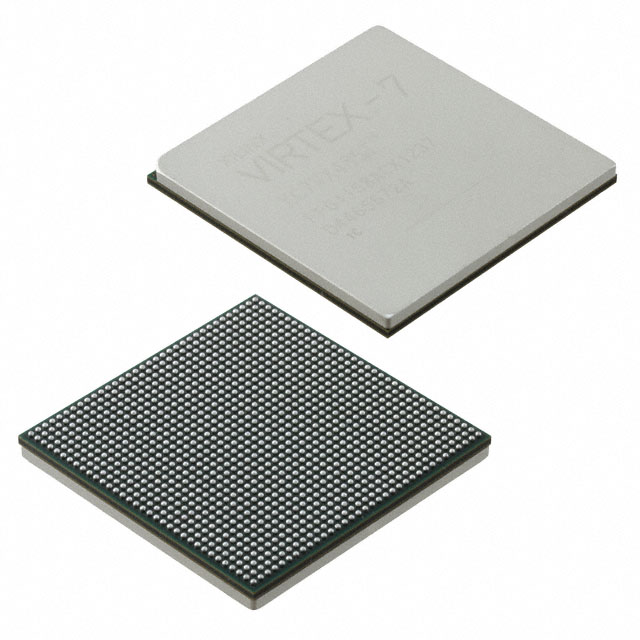
IC કેરિયર: સામાન્ય રીતે, તે ચિપ પરનું બોર્ડ છે. બોર્ડ ખૂબ નાનું છે, સામાન્ય રીતે, તે 1/4 નેઇલ કવરનું કદ છે, અને બોર્ડ ખૂબ જ પાતળું 0.2-0 છે. વપરાયેલ સામગ્રી FR-5, BT રેઝિન છે, અને તેની સર્કિટ લગભગ 2mil/2mil છે. ઉચ્ચ-ચોકસાઇવાળા બોર્ડ માટે, તે તાઇવાનમાં બનાવવામાં આવતું હતું, પરંતુ હવે તે મુખ્ય ભૂમિ પર વિકાસ કરી રહ્યું છે.

HONTEC પાસે 30 મેડિકલ PCBA પ્રોડક્શન લાઇન્સ છે જેમ કે Panasonic અને Yamaha, Germany ersa સિલેક્ટિવ વેવ સોલ્ડરિંગ, સોલ્ડર પેસ્ટ ડિટેક્શન 3D SPI, AOI, એક્સ-રે, BGA રિપેર ટેબલ અને અન્ય સાધનો.

અમે PCBA થી OEM/ODM સુધીની ઇલેક્ટ્રોનિક ઉત્પાદન સેવાઓની સંપૂર્ણ શ્રેણી પૂરી પાડીએ છીએ, જેમાં ડિઝાઇન સપોર્ટ, પ્રાપ્તિ, SMT, પરીક્ષણ અને એસેમ્બલીનો સમાવેશ થાય છે. જો અમે HONTEC પસંદ કરીએ, તો અમારા ગ્રાહકો અત્યંત લવચીક વન-સ્ટોપ પ્રોસેસિંગ અને મેન્યુફેક્ચરિંગ સેવાનો આનંદ માણશે.

HONTEC એક વ્યાવસાયિક PCB એસેમ્બલી વન-સ્ટોપ સર્વિસ પ્રોવાઇડર, PCB ડિઝાઇન, કમ્પોનન્ટ પ્રોક્યોરમેન્ટ, PCB ઉત્પાદન, SMT પ્રોસેસિંગ, એસેમ્બલી વગેરે છે.

કોમ્યુનિકેશન PCBA એ પ્રિન્ટેડ સર્કિટ બોર્ડ + એસેમ્બલીનું સંક્ષિપ્ત રૂપ છે, એટલે કે PCBA એ PCB SMT, પછી ડિપ પ્લગ-ઇનની સમગ્ર પ્રક્રિયા છે.

ઔદ્યોગિક નિયંત્રણ PCBA એ સામાન્ય રીતે પ્રોસેસિંગ ફ્લોનો સંદર્ભ આપે છે, જેને ફિનિશ્ડ સર્કિટ બોર્ડ તરીકે પણ સમજી શકાય છે, એટલે કે PCB પરની પ્રક્રિયાઓ પૂર્ણ થયા પછી જ PCBAની ગણતરી કરી શકાય છે. PCB એ ખાલી પ્રિન્ટેડ સર્કિટ બોર્ડનો ઉલ્લેખ કરે છે જેમાં તેના પર કોઈ ભાગો નથી.